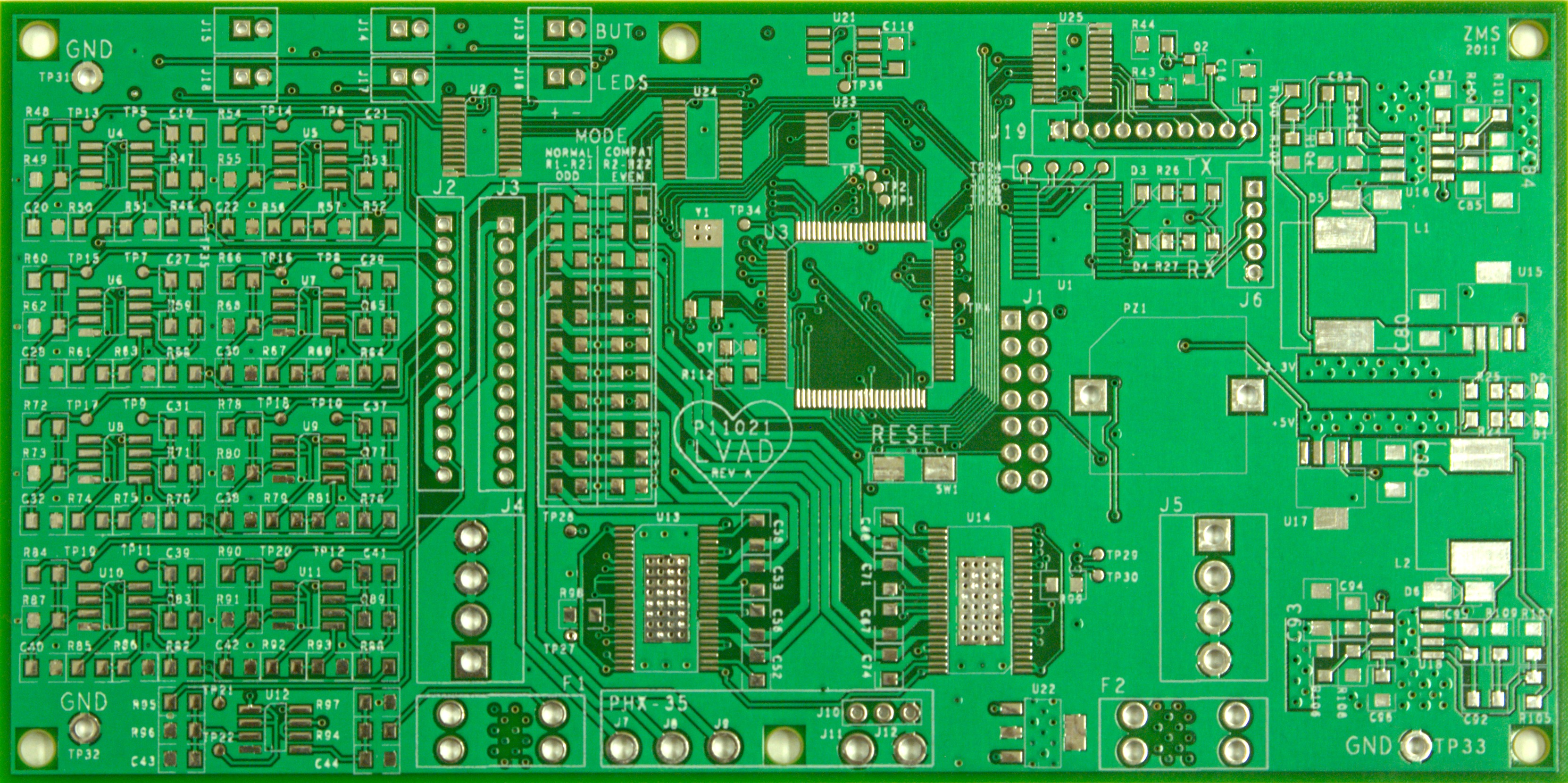
PCB Layout 6 Layer: High-Performance Electronics SECRET! Pcb layout optimization for emi and emc
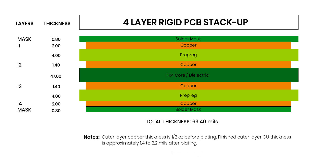
If you are searching about Guide to Multilayer PCB Layer Stackup and thickness - JHYPCB you've visit to the right web. We have 25 Pics about Guide to Multilayer PCB Layer Stackup and thickness - JHYPCB like 6 Layer PCB Prototype & Stackup | JLCPCB, 4 Layer PCB Layout Tutorial, Stack-up design, and Cost of manufacturing and also PCB Stack-Up Guide & Examples | San Francisco Circuits. Here you go:
Guide To Multilayer PCB Layer Stackup And Thickness - JHYPCB
 www.pcbelec.com
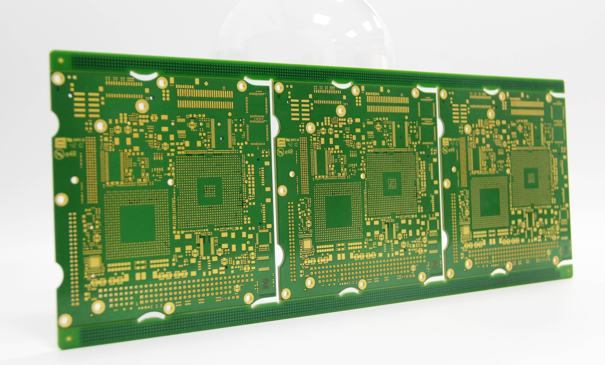
JLCPCB High-precision Multi-layer PCB Extended To 8-20 Layer
Pcb Design Layout Guidelines Pcb Layout Guidelines For Design
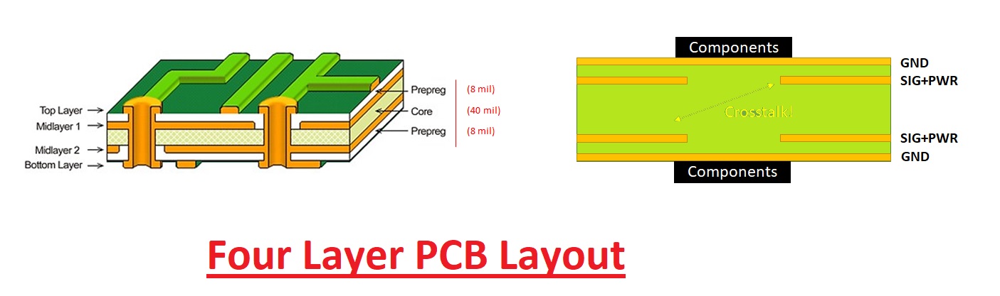
 pcbways.pages.dev
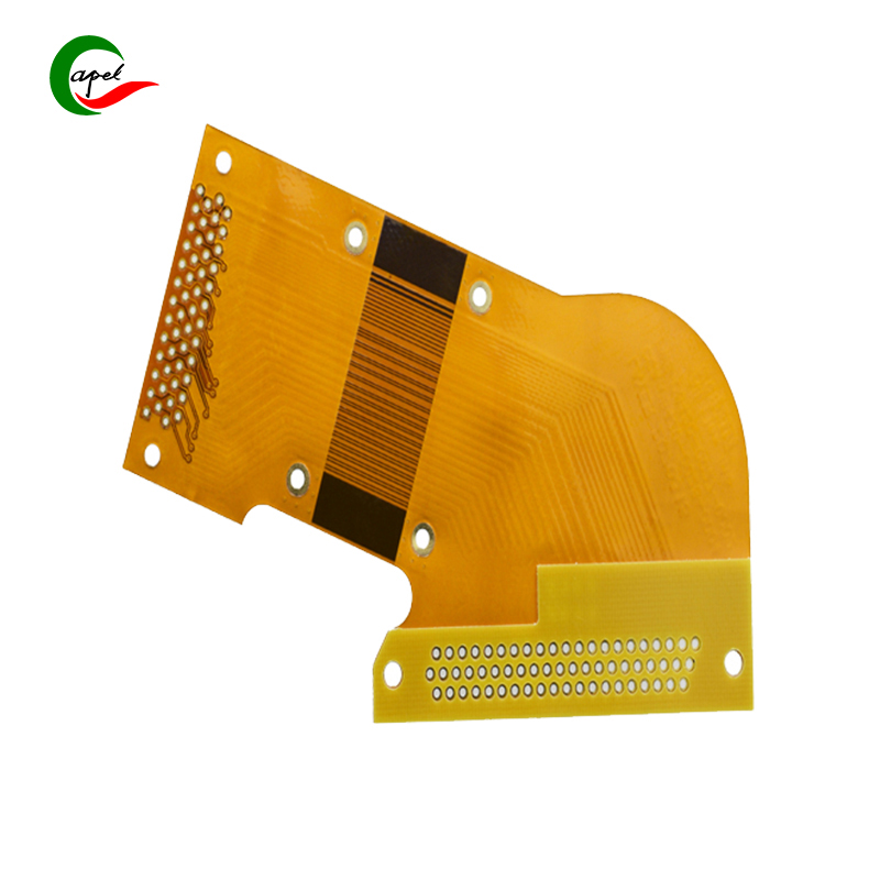
Supply 4 Layer High Density Flex-Rigid PCB Consumer Electronics
 www.multech-group.com
What Is The Layer Of A Pcb - Vrogue.co
 www.vrogue.co
8-Layer PCB Stack-up: Maximizing Electronic Performance - MorePCB
 morepcb.com
Hardware Design With The RP2040 Part 2: PCB Layout Rp2040 Kicad 6
 pcblites.pages.dev
PCB Layout Optimization For EMI And EMC
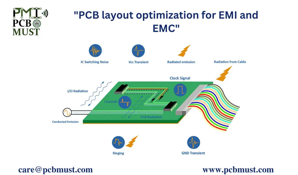 pcbmust.com
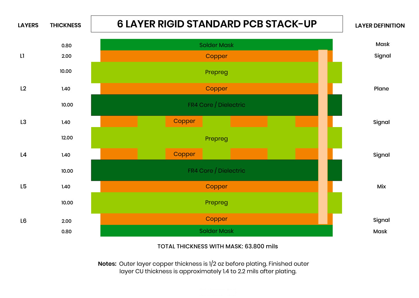
Guide To Six-Layer PCB Stack-up And Manufacturing Process | Viasion
 www.viasion.com
4 Layer PCB Layout Tutorial, Stack-up Design, And Cost Of Manufacturing
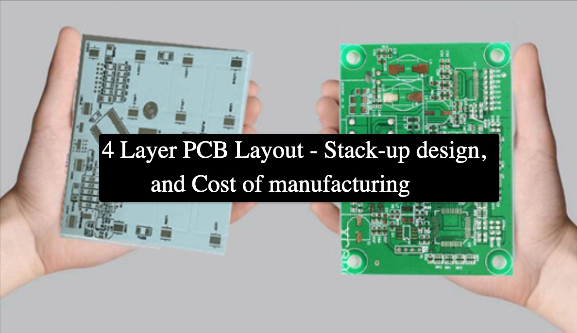 absolutepcbassembly.com
Supply 4 Layer High Density FR4 PCB Board For Security Surveillance
 www.multech-group.com
PCB – SuperHouse Automation
 www.superhouse.tv
pcb smd surface superhouse pcbs circuit tag finishes
PCB Stack-Up Guide & Examples | San Francisco Circuits
 www.sfcircuits.com
What Is The Better PCB: 2 Layer Vs 4 Layer PCB?
 www.pcbmay.com
China Quick-Turn PCB Prototyping 6 Layer High-Density Multi-Layer
 www.capelfpc.com
PCB Insulation: Non-Conductive Layers For Separating PCB Electrical
 www.ourpcb.com
6 Layer PCB Prototype & Stackup | JLCPCB
 jlcpcb.com
2 Layer PCB Stackup: Structures, Advantages And Applications | Viasion
 www.viasion.com
Unleashing The Power Of 16-Layer PCB - Characteristics, Advantages And
 www.pcba-manufacturers.com
Pcb Layout And Thermal Design Techniques For High Den - Vrogue.co
 www.vrogue.co
Single-layer PCB And Its Types - The Ultimate Guide 2022 - IBE Electronics
 www.pcbaaa.com
Our Hints For High-speed PCB Design
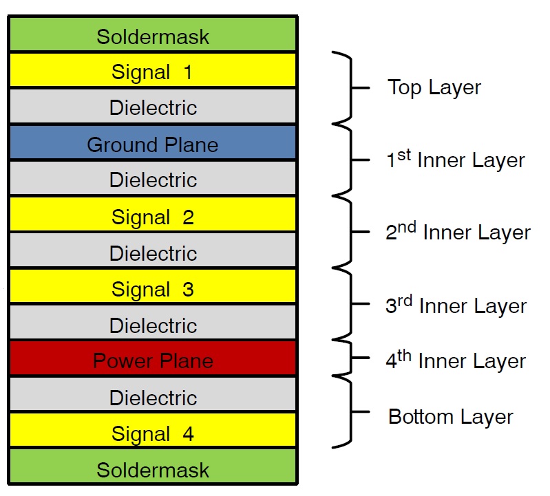 www.proto-electronics.com
stackup pcb layers example high speed design hints name our figure planes
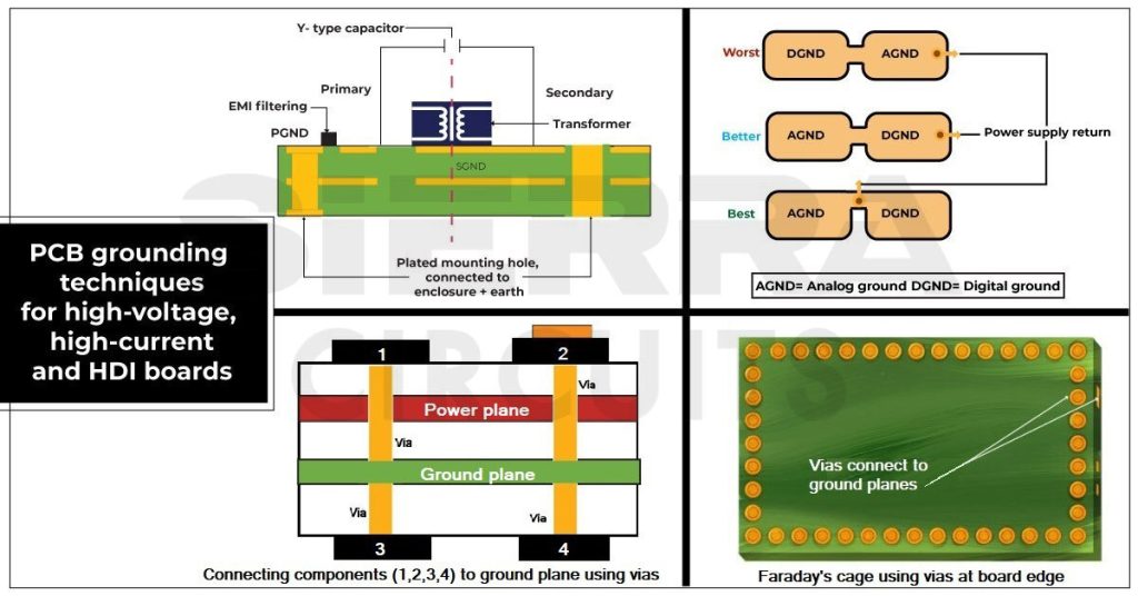
Grounding Pcb Crystal Layout Electrical Engineering S - Vrogue.co
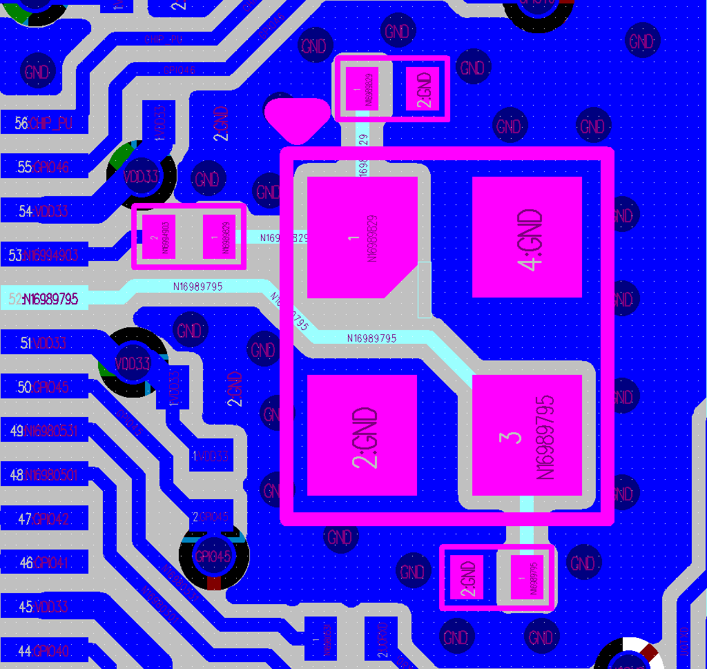 www.vrogue.co
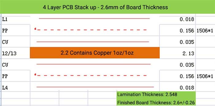
Pcb Thickness 4 Layer Pcb Stack-up – Pcb Hero
 pcbways.pages.dev
High Performance Thin Layer Chromatography [5]
![High performance thin layer chromatography [5]](https://www.researchgate.net/profile/Rekha_Priyadarshini/publication/289525226/figure/fig3/AS:315255268888578@1452174121518/Figure-4-High-performance-thin-layer-chromatography-5.png) www.researchgate.net
www.researchgate.net
chromatography layer thin
What is the better pcb: 2 layer vs 4 layer pcb?. 6 layer pcb prototype & stackup. Grounding pcb crystal layout electrical engineering s